| EN CZ PL | ||||||||||||||||||||||||||||||||||||||||
|
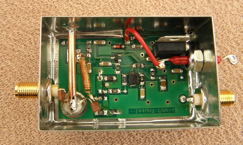
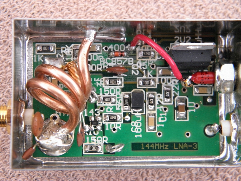
Due to growing of electromagnetic smog on all bands, my son OK1TEH push me for a long time to arrange him some more robust 70cm LNA, than the old LNA with classic MGF1302 and NF abt.0,45 dB was. Because on the web is a plenty different designs of LNAs and many designers just repeats pros & cons of the previous designs and often they are published it as they original invention, it makes a bit problematic to find real reliable and repeateable construction, which has been made by many OMs with success and which is not extremely sophisticated for home built. The next - and not the last criterion - is as best as possible input matching, because such LNA is notably used behind some piece of cable and not directly on the antenna dipole. Selection of transistor was relatively simple: due to accessibility, price and performance evaluation has won well-known ATF 54143, which is possible to buy from many distributors. It turn me to the second issue, input reflections. Final decision was to take LNA by OZ1PIF, because such LNA is used by some EME enthusiasts and it is on the top improved of well-proven PA3BIY design, described in Dubus (what is considered as some mark of quality) and OZ1PIF remake design has been sold in hundreds of pcs with success. So - we considered this LNA as fully debuged design. It has been supported by fact, that some ops used this LNA as base for their own construction - for example Zdenek OK1DFC, made 23cm LNA which used RF part design by W6PQL and from PA3BIY circuits has smart BIAS circuit for automatic adjustment of working point of ATF transistor... And for last, but not least the OZ1PIF design won due to complete PCB design in Gerber file, redrawed by OZ3SW, which gives us opportunity save the time and chance to arrange professional PCB without any necessity to design your own PCB.
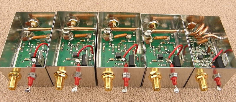
Amplifiers were revived - at first in DC (ATF's current was piece by piece between 53 to 58mA) an then by spectrum analyzer. The maximum gain has been adjusted (in average it was some 1dB below OZ1PIF results) and input reflections were measured. Such value was not so brilliant as in the OZ1PIF article, but I got after a small detune -20dB, which was fine. Everything works well, no troubles, all works more-less perfect. No changes, no replacements, no medicine were needed. Simply good design, which works in first setup. BTW: requested copper wire for coil with 2,5mm diameter you will find as central conductor in H1000 cable, hi.
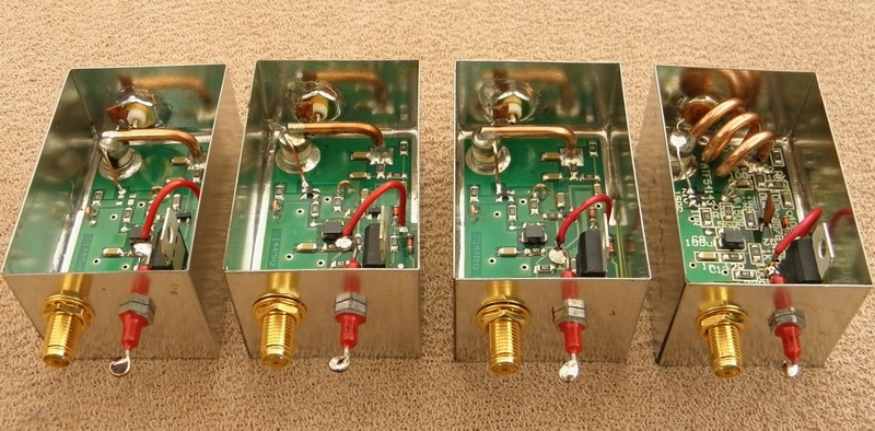
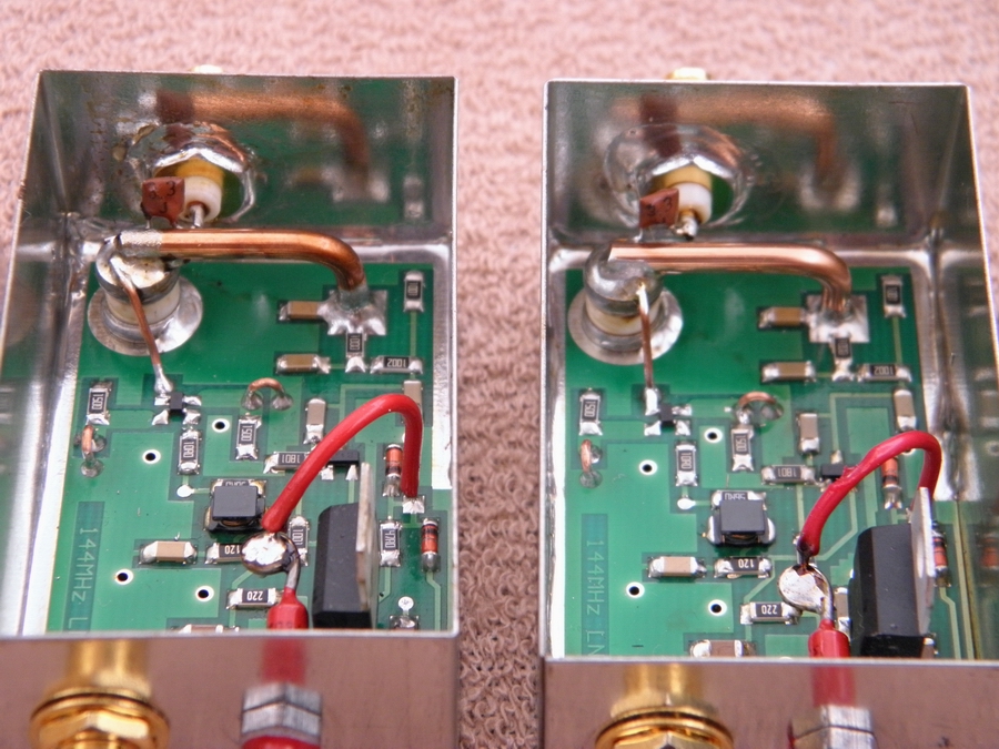
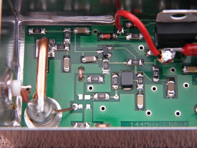
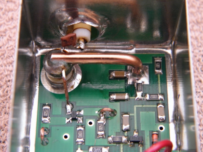
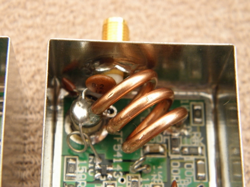
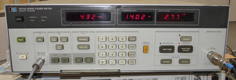
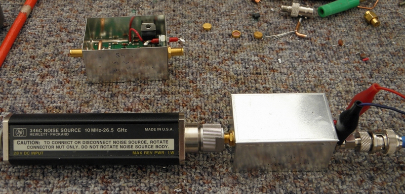
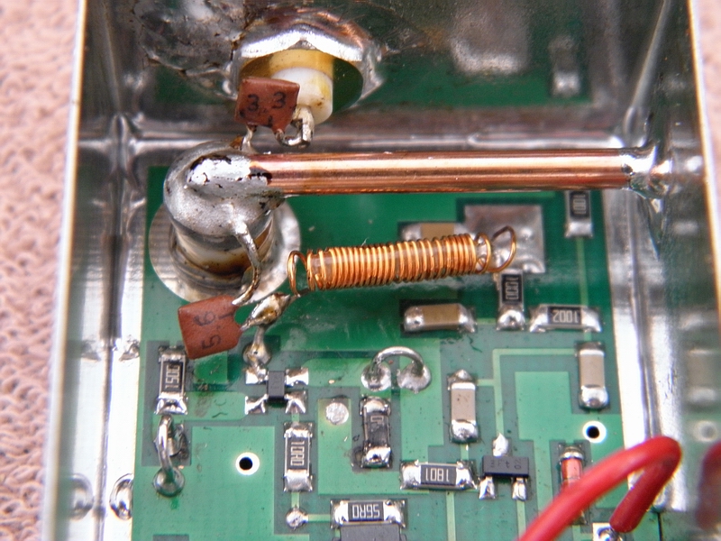
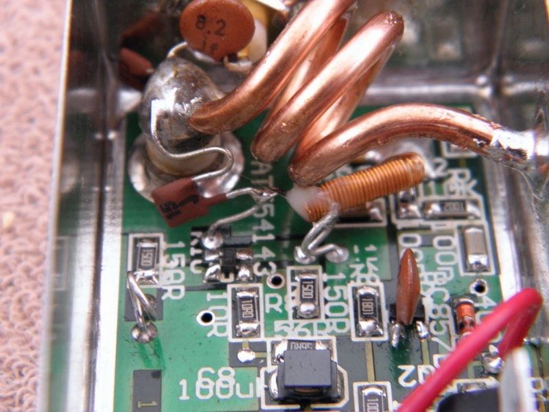
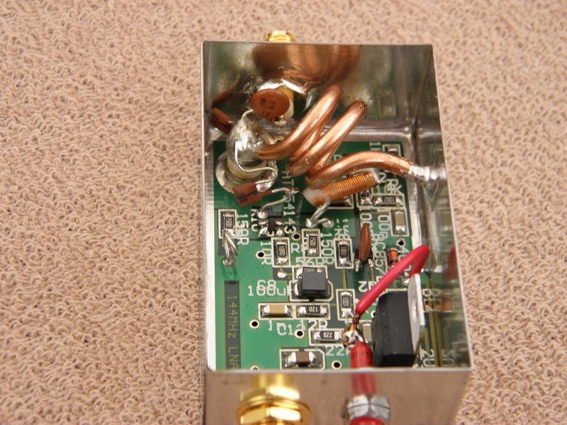
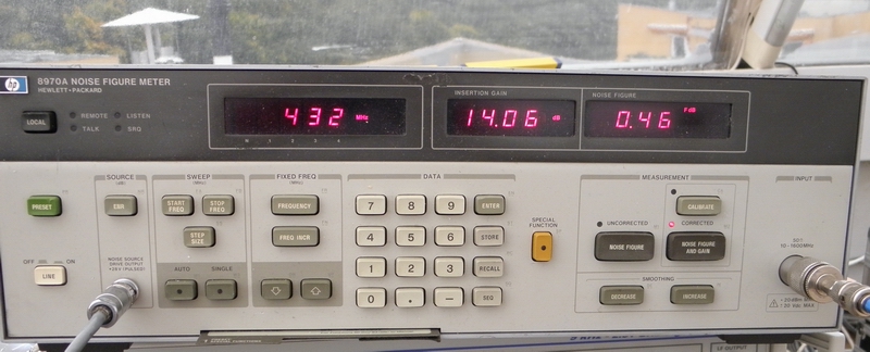
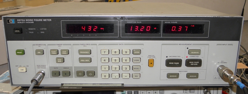
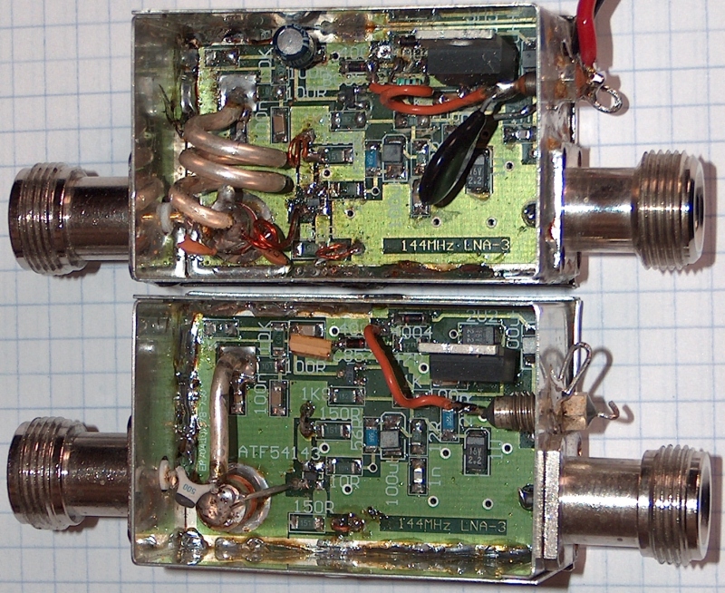
And then get started a drama. I install a bit older, borrowed noise figure meter by HP, and when the machine was heated up, I completed calibration and start measurment of these LNAs. First result was shock: 2,4 dB ! Some retuning helps only in the range of hundredth of dB. The next was 1,63 dB, third 2,75 dB... the fourth as well as! Because morning is wiser than evening I go to the bed. After that I was busy for 2 days. But did not forget it and consider more hypothesis, like bad PCB material (but it was refused immediately, because one of LNAs was made on original OZ1PIF plate), bad transistors (however they were from different suppliers), bad SMA connectors (Chinese but with teflon and wheni nterconnected, the loss was below 0,1dB), bad capacitors trimmers (but the same in the old LNA resulted with 0,45dB NF). So no clear mistake were observed. For final, as usual, help me the mathematics. Result of my primitive analysis of the input circuit was relatively clear - when setup the computer modeling and put there value of each component include loss, the most important influence has blocking capacitor C4 on the "cold side" of the input coil L1. In case of real tangens delta of standard ceramic 1nF SMD capacitor was clear, that on 432MHz we can not await any miracles and the input noise factor will be impaired. Beside it as well as R1 (100R) resistor will not decrease loses of resonance circuit, not very well blocked by C4. Unfortunately I was not able made a replacement of this C4 by low loss SMD power capacitors (for example by ATC), because I have in my shelf few of them with values below 100pF only. So the improvement of the circuit was needed ;-) The best RF blocking capacitor is no blocking capacitor. Galvanic direct interconnection has much lower loss, parazitic serial resistance would be quite low. And when the gate of transistor shall be separated from the ground, why not to do it on higher impedance, where the loses of coupling capacitors are negligible. The next reason for reconstruction of LNA input is the issue of resistance against lightning. In the original connection it is more-less sure, that the ATF must be destroyed, because relatively high impednace of R1 + R2 + R3 can not prevent voltage peak, transferred to the gate via capacity of C1. BTW, such design failure could be observed in more LNAs, what resulted in rumours, that ATF54143 is extremely sensitive for static electricity. Not bad design of transistor could be blamed for it - bad design of LNA is the reason.! I will not bother you by too long story - the modified LNA design is clearly visible on these pics:
The input resonance curcuit is on the "cold" side grounded and from the "hot" side is FET Gate connected via added coupling capacitor - by empiric testing of 5 LNAs has been setup the optimum value about 5.6pF on 432 and 10-12pF on 144MHz. Bias voltage is to the FET Gate connected through air choke. This choke is wounded by enameled wire cca 0,25mm diameter on the 2mm spike (30 threads). However few pics will be better, than long description:
However in practice we are not the listening to the Noise factor or to IP3, but by ears. And any LNA must be connected somewhere. And such measurment was not so optimistic, like original OZ1PIF's construction. My LNAs, optimized to the best NF, were input attenuation reflections only 6 to 9dB... When optimized by retune of the capacitor trimmer to best reflections (at least -20dB) will be NF degraded to cca 0,7 dB. It is logical. This PHEMT device will have "naturally" minimum noise always in the other point, than power matching, maybe with a bit better situation on 23 and 13cm bands, were would be possible to arrange closer power and noise matching by relatively broadband input circuit. But such input circuit is not suitable for lower bands. I'm not alone, who is convinced of it... Broad band matching is fine for EME however for contest station such circuitry would make EMC troubles with "out of band" signal, particularly second order intermodulation from two DVB-T transmitters may create heavy QRM on 23cm. Some contesters already know well such issue, hi. What is better for 2m and 70cm matching? Noise of impedance one? Optimization is a result of LNA position and in practise could be the result of total noise of reception chain even better with better impedance and worse noise matching, than opposite. BTW check this table of loss due to missmatching and you have what thinking of, hi. If you want to construct such LNA in your shack and no noise figure meter is available, do not be sad. Impedance matchin is the same as LNA adjustment for best gain. Optimized Noise figure you will get when the input circuit is detuned to the higher frequency until the gain on 432MHz has decreased by 0.9dB. It was very same for all 70cm LNAs, which I made. Two meter's LNA have similar behaviour, but I did not made series of 2m LNAs and I can not generalize gain decrease influence and best NF point. Results of my measurments:
LNA with this modification will be for sure more robust against lightning voltage peaks as original OZ1PIF version, or similar SM6FHZ modification. If you will not adapt such LNA as recommended in this article, try rather YU1AW or F8KTH designes - the second one even on original PCB. When you calculate to use protective Schottky diode as described here, NF would be worse by cca 0,15 dB. Intermodulation resistivity of this modified LNA by OZ1PIF was not measured, I have not two good programmable generators, so I will trust producer datasheet. Modification of input should not be worse, than original design. BTW, LNA with very high IP have in hamradio practise importance only in reception setup, when are observed EMC troubles from "out of band" strong interference. Then is recommended to use LNA, followed by circulator and BPF. In case of interference "on the band", LNA's IP3 is not so important, because significant role will have IP of receiver behind LNA. More on this issue here. Conclusion? It is the next confirmation, that better is to measure, than trust. Eve "well proven" design could not to have declared performance. Some web pages tolerates even more, than paper... And only "marginal" mistake in construction or in description of components type may resulted by very different results Thats all. Pleasant time during construction of some suitable LNA, transverter or SSPA wish you OK1VPZ
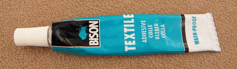
Note: for mechanical fixation of small RF chokes (like for ATF54143 gate) I have good experience with "textile fixation glue", which you may buy in local Supermarket. No influence to the RF performance of choke were observed (like negative influence to Noise Figure of such LNA).
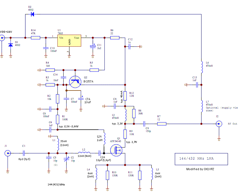
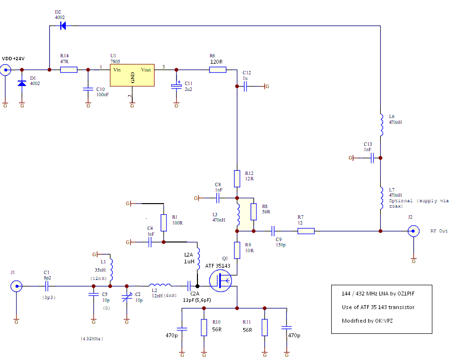
Amendment Since time of first publication of above article abt. OZ1PIF's LNA I made next two units. Beside it I got several reactions from others with info related to the BIAS circuit oscillation a asks for alternative FETs. Let me to have few words on such theme: a) At first below is modified schematics of LNA, reflected described changes. Original schematic by OZ1PIF is here:
b) But one ATF 54143 LNAs were in practise in the matter of intermodulations much worse, than others. Local strong stations in VHF Contest were observed with splatters, however their signal, received by other LNA was OK. Such interference had correlacion with strong signal from the local transmitter, where are located 10kW ERP FM radio and DVB-T transmitter. Why? Solution of this mystery proposed Josef OK1TKP - it was oscillation of the Bias control loop. When measured by oscilloscope, on 2 LNAs (from total 6) were observed on the collector of PNP transistor BC857 low frequency oscillations, some 200mV peak to peak, what of course damaged intermodulation performance of LNA. Such wobbling has extinguished by tantal capacitor 10uF between transistor collector and ground (parallelly to C7). But it just helps and better is remove the reason - too high current gain of that transistor (H21e), much higher, than recommended than BC857b from OZ1PIF's components list and it would be BC857a, or BC856a with lower gain (check the symbol 3A, resp.3E on transistor body) and only after that add for sure parallelly to C7 the tantal capacitor. It seems, that such problems had OZ1PIF as well as (but he did not say anything about it), because on his LNA pics you may see in the same place electrolytic capacitor and he hes in the list of components anoter transistor, than in the schematic. For final - I would suspect, that original input circuit of LNA was more sensitive for such control loop wobbling, than after modification. It resulted by in p ractice relatively good intermodulation robustness against strong "out of band" signals, for example in OK1TEH's 70cm RX were observed much lower broadband noise from local DVB-T transmitter in case of use ATF54143 LNA compare older MGF1302 LNA.
c) We try the test of use alternative transistor - cheaper ATF 35143, which is in comparison to original ATF 54143 a bit worse in the intermodulations, but even a bit better in Noise Figure, albeit I cant confrm better NF after replacement of it in the LNA, but for "out of contest" traffic this transistor could be acceptable replacement of more expensive ATF 54143 and it helps...But ATF 35143 has in comparison with original transistor another recommended working status (2V and 15mA versus 3V and 55mA) and due to it was needed to make further modifications:
Results were not measured on more units, so just for info - gain was a bit lower (cca 14dB on 70cm), Noise figure abt 0,45 dB.
The Noise figure of LNA (with any of the above mentioned transistors) could be even a bit better by application of higher Q input circuit (like lambda/4 resonator from piece of half inch cable). But such idea is waiting for your tests, hi. That is to the OZ1PIF's LNA construction. Maybe it helps to someone. 73 de OK1VPZ (2010) Additional note (2018) here. |