|
Why isn't a good idea to use the impulse modes transistors at ham radio SSPA? Many days passed before I finally decided to write a next article for our "HW corner", but I hadn't been able to avoid employment and family responsibilities which have been absorbing almost all of my free time withing last year.. So I'm happy that I finally wrote my "few cents" to the 23cm SSPA topic. The highly experienced radio amateurs have been considering and looking for new high power transistors for L-band (about 1090 to 1400MHz) for over 25 years. But these transistors seems to be (unfortunately) determined to use just for impulse operation, because they are mostly produced for radar applications - mostly for planes secondary radar application and/or maritime use. At the beginning the first generation of these L-band transistors were only bipolar designed for common base use which was next trouble for linear application. As the result the number of real hamradio SSPAs based on such transistors was pretty low and if such a PA was completed, designer did not boast the estimated results. It would certainly be interesting to look at why.
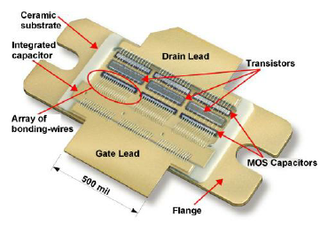
When the first generation of GSM base stations with semiconductor PAs became obsolete and forwarded to waste, the radio amateurs found their way to the discarded parts and re-tuned them - someone more, someone less successful, to 23cm. Of course lot of these constructions were based on trial and error procedure. I doubt that anyone had ever had an access to a datasheet of the transistors used at these BTSs, such as BLV958 including precise description of the input and load impedance values at frequency of 1.3 GHz. After some time these bipolar transistors (for 900 MHz band) were replaced by LDMOS transistors and radio amateurs, of course, looked for them again. However, such as hamradio amplifiers based on LDMOS transistors were done hurriedly and carelessly, better said "in a pure amateur way". Of course, thanks to endless patience and lot of spent time and many destroyed transistors, it has been possible to develop the reusable constructions, but the solution remained far from the ideal one. The reason was obvious, the transistors such as popular MRFE6S9160H were operating at frequencies 30% higher (1296 MHz) than they were intended by the manufacturer for, which caused the problems with their coupling at the amplifiers particularly designed for high power (EME) operation. Among the amateurs, the input and load impedance values became to be known (chaps from Russia did lot of work on it), however due to claims of US4ICI these data were rather obtained only by the reverse engineering (mostly from the DF9IC's design), so it's uncertain how much we can rely on these data anyway. A lot of people have been able to build up and successfully operate such a EME PA, others not. Some of these problems I discussed at the following article. An another problem of such a PA design is the transistor's BIAS current dependency on the temperature, which isn't fault, but only an attribute, however the results is a requirement for a temperature compensated source of bias in case that we want use these transistors at full power output. Other designers decided to do it in the another way. Michael, DB6NT has introduced a series of SSPA modules with the PTF141501A transistors which were originally intended for digital broadcasting DAB at L-band (frequencies ranging from 1.45 to 1.5 GHz). And he also had a problems. The first generation of these SSPA series wasn't able to deliver full power for a long time, due to problem with high temperature and short lifetime. The situation improved with the the arrival of the new transistor PTF141501E with an improved thermal transition between the semiconductor chip and the transistor case. An another great improvement in such a DB6NT's PA was replacement of the aluminum housing by a copper pad. As we used such a PA at our radioclub, I have made (based on discussion with Michael) some excel-sheet table with the hidden calculations to figure out the possibilities of the better transistors cooling. How you can see at this link, even a slight change in temperature resistance inside the transistor has an big impact on the achievable output power of such a SSPA! Infineon began producing even more powerful mutation of a such a transistor (PTFA142401E) that would be even better for amateur radio usage at 1296 MHz, however at the meantime the T-DAB broadcasters at L-band have moved to more efficient digital radio broadcasting at the III.rd TV band channel because these frequencies provide much better coverage for the mobile traffic, so nowadays such a nice transistor isn't manufactured by Infineon anymore. Of course, they are an alternatives offered by other manufacturers. For an example, the transistor MRF7S16150HS or the BLF647P offers basically the same thing and what have to be said, it's always easier to pull the transistor's original frequency downwards than upwards. And while the series of transistors working between 1.8 to 2.1GHz are wide spread, amateur radio designers have fun to take care of. But the time has changed. No one has free time left, human society is rather in a relational crisis, while the material for some experimental hardware constructions is a general surplus, and so, if we want to have a little free time for our hobby, we have to look for the reliable solutions. Or, at last, for the transistors which are perfectly designed for what we need, because life is too short for discovering a dead end streets (just like life is too short for QRP at VHF ;-). And the time is also changing in the branch of RF component manufacturing. The NXP Group has acquired the production of HF power transistors in the United States and has joined together with Freescale (formerly Motorola). Motorola itself has already reoriented to manufacturing of another type of electronics. Interestingly, NXP's production of VF transistors, which we have known as NXP in the last few years (and even earlier as Philips) in the last few years, has also been split too and Ampleon company was established. For us Europeans, it is only sad that the knowledge of the development and production of RF power transistors has moved from Europe to the American continent... But back to the topic. Radio amateurs would like to buy high power RF transistors for their PAs, which are easy for coupling, inexpensive and very robust, because radio amateurs do not handle with them with kid gloves. But we also need to focus on other changes that the time brings, and especially on the technical parameters.
The changes in recent years resulted, on the one hand, to the end of the production of many reliable, proven and useful transistors, but in many cases, as well as, interesting development projects. But that's the case of companies ruled by the crazy economists... The fact that such a transistors are still on the marked is the result of the diligent work of Chinese electronics. But let's go back to the 23cm PA: The RF transistors for this band today are dominated by transistors for higher supply voltage (50V), because higher power means higher load impedance and thus smaller losses in matching circuits. Such a L-band transistors are more and more based on SiC (Silicon - Carbide) and GaN (Galium Nitrid) materials, because these materials tolerate a higher operating temperature of the semiconductor chip and generally have better performances than the existing silicon transistors (especially for military requirements). So if UHF radio amateurs want to keep their gaer up to date (quite good) overview and keep their equipment at the time level, they have to pay attention to them. One of the representatives of modern transistors suitable for the 23cm band is, for example, MMRF1005H or BLF6G13L-250P, and we would certainly find a number of analogical transistors from other manufacturers. These transistors are designed directly for the required band, they are able to deliver RF power output over 200W, input and load impedances are available and - which is very important! - these transistors are (also) intended for CW operation mode! Please be aware that CW means "Continuous carrier", ie, continuous carrier is not telegraph traffic! Thus, such a operation is very similar to FM mode or digital FSK (eg. WSJT). The telegraph operation does not require such a big demands on PA compared to an amplifier, which is designed for FM or WSJT operation (this corresponds to a "key down" test). Telegraph operation contains dots, dashes, and spaces when PA "relax" and does not produce heat (or so much heat). And the heat is what it's going on! Of course, semiconductor manufacturers are also producing plenty of beautiful components for pulse traffic in our 23cm band or its surroundings frequencies, and many radio amateurs want these components (like MRF6V12500H or BLL6H1214-500 or PTVA127002E). Is possible to use these transistors to construct SSPA for the 23cm band? "Yes we can", but... Please
note one important number in the datasheet called "thermal resistance"
Junction - case, or RθJC: it is a number written in °C/W or K/W and it
indicates the thermal resistance between the semiconductor chip and the
case of the transistor. In practice, this resistance for high power RF
transistor typically is range between aprox. 0.2 and 0.8. For an example,
if the value is 0.5, this means that if the heat transfer passes the 1
Watt of heat output, the chip temperature increases by +0,5 °C. So, let's
make an analyze: if the heatsink temperature of the transistor case is set
for example at 60 °C, the temperature of the transistor's case will be
higher by the thermal resistance between the cooler and the transistor's
case. Now let's estimate the resistance between case and heatsink at about
0,2 °C/W. For a
PTVA12700E transistor
(which is operating
in pulse mode and having an internal thermal resistance of 0,36 °C/W) the temperature of the semiconductor chip will be calculated as
follows: Now let's look at some other transistor designed for CW operation, such as the above-mentioned MMRF1005H, so that we can compare at which chip's temperature (of the semiconductor) transistor operates in the "continuous carrier" mode. RθJC is 0,42 and with Pout 235W the transistor has an efficiency of 53%. All this at (a case) temperature of 77 °C. So power consumption will be about 443W, and 208W of heat shell be removed from the chip. If the transistor housing temperature is 77 °C, the chip temperature will be: 208 x 0,42 = 87,5 ° C + 77 ° C = 164 ° C. And this is a significant difference compared to the previous transistor if it was operated in a "catalog" pulse mode with a duty cycle of 12%! Let's assume that the transistor PTVA12700E will also operate in CW mode with a chip temperature of 164 °C. What RF power output can we expect of it? For a thermal gradient of 164 - 70 ° C (see datasheet) and a thermal resistance of 0,36 °C/W we will be able to transfer about 261W (94 / 0,36) of the heat output from the chip. If the transistor will have an efficiency of 56% even at this lower power (the output matching circuit would have to be adequate to this reduced power because the transistor will have a different load impedance than with the 700W of RF power output), we can expect from the transistor power input of 593W (261 / 0,44 ) and output power around 332W (593-261). This is only slightly more powerful than the above-mentioned 250-watt transistor. So as if we want more RF power output from the PTVA12700E transistor (such as the 700W device) and increased the driving, we will definitely destroy the transistor. Such a transistor is usable for SSPA, but we can not expect any amazing power output or better said "HF miracles"! But it has even one more pitfalls: the input and output load impedance values listed for the 700W RF power output at datasheet are not the same like for the RF output power of 332W. As the result we could expect, that, during the real PA operation, the impedance matching will not be optimal, which will make even further increase of the chip temperature. What temperature should be considered and calculated for a transistor chip if we're designing a new SSPA? Frankly said as low as possible. One old rule says - If we increase the temperature of the semiconductor chip by 10 °C, its reliability will drops down by 100-times. Silicon transistors should not be operated at chip temperatures higher than about 160 °C, and for transistors older than about 10 years, only around 150 °C (if we don't want to shorted the transistor's life rapidly). It's because the fact that increased chip temperature also reduces its permissible collector loss and resistance against to bad adaptation. I'd recommend to check the graph (with an oblique corner) at the transistors' datasheet showing the safe area of it's operation. It is quite interesting why some manufacturers don’t show the safety area graph as a part of datasheet (probably for marketing reasons) and others attach only a short note such as: "Total Device Dissipation @ TCase = 25 °C: 476W, derate above 25 °C by 2,38W / °C" as it's written at Freescale datasheet for the transistor MMRF1005H. The higher temperature of the semiconductor transition (approx. 200 °C) will be acceptable with the new GaN transistors, but so far there are not wide spread among the radio amateurs because of their high price.
Let's get back and take a short look at the probable chip temperature of well known and popular 1 kilowatt 2-meter transistor MRF1K1250: At output power 1250W, the efficiency is equal to 78% and the thermal resistance is 0,15 °C/W and the temperature of transistor housing is about 63 °C. It can be expected that the chip temperature will be only 116 °C in such a case! So it isn't a surprise that that such a transistor will lasts bad handling indeed!!! Maybe you would be interested how it's the situation of the 23cm SM4DNH's SSPA which was presented by OK1DFC? The transistor BLF6G13L-250P will have in operation time chip temperature just below 136 °C (if it is actually optimized for the real impedance of the transistor) for 250W RF power output, efficiency of 56%, thermal resistance 0,26 °K/W and transistor housing temperature of 85 °C. Now let's consider by yourself what performance you could afford to get from your home semiconductor PA if you think about the facts presented in this article! The efficiency and thermal resistance inside the transistor determines its lifetime!
Conclusion I outlined the calculations of heat transfer conditions for the solid state PA. The practical result is, however, also dependent on the heat transfer between the transistor housing and the heatsink, the heat resistance of the heatsink to the cooling air and its flow rate, the shape of the radiator ribs on its size and material. But that's another topic, and maybe I'll write about it next time. For the first info, just keep in mind that the aluminum radiator does not have the reason to enlarge it over the dimensions of about 20 x 20 cm if it has slim ribs and base strength of about 1 cm. If it is larger, the thermal resistance of the aluminum is so great that a larger radiator will cool at the edges very little or not at all. Consequently, copper heatsink or at least a strong copper plate that spread heat across the aluminum cooler are often used for critical applications (like EME). It is then advisable to solder the power transistors on such a copper plate directly to minimize the thermal resistance between the chip and the cooler or even use the water cooling.. Don't be confused by any means above and consider yourself each step carefully. This article was written just as a friendly note and for discussion, not as an specific instructions which might lead to damage of your new SSPA project. Please don't forget that anything you are doing is only at your own risk. 73 ok1vpz The article was translated by Matej, OK1TEH |